


Odisha is emerging as India’s next semiconductor hub with new policies, ESDM clusters, skill centres, and a ₹4,009 crore chip investment
OdishaPlus Bureau
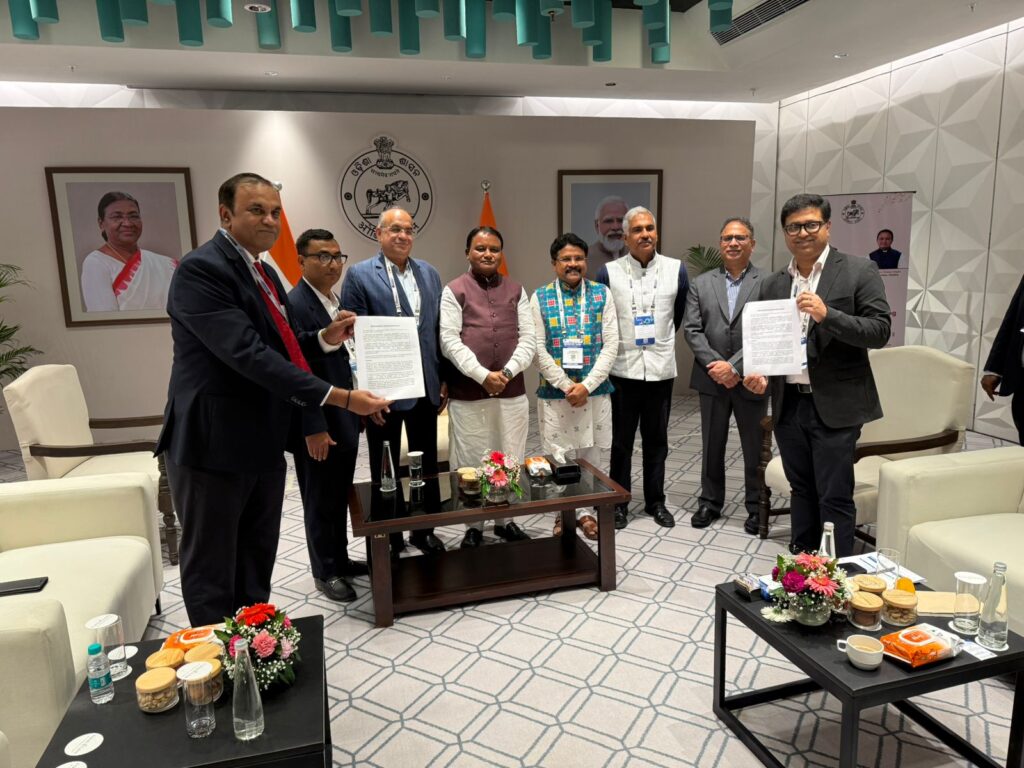
Odisha is poised to emerge as the next big destination for semiconductor and electronics innovation, chief minister Mohan Charan Majhi said on Tuesday as he inaugurated the state’s pavilion at SEMICON India, 2025 in New Delhi. The Odisha Pavilion spotlighted the state’s growing semiconductor ecosystem, backed by progressive policies, modern infrastructure and a skilled talent pool. The CM’s remarks came as Prime Minister Narendra Modi launched the country’s first indigenous chip, a milestone that Majhi described as ‘truly inspiring’ in a social media post.
Majhi congratulated PMEC Berhampur for developing the high performance multiplier IC and lauded NIT Rourkela’s contributions to the Made in India chip initiative through its VG amplifier and sensor circuit and present encryption core. “These achievements reflect the innovation nurtured within our institutions and Odisha’s growing role in India’s semiconductor journey,” Majhi posted on X, adding that the state’s bold policies and investment-ready infrastructure are positioning it as a future hub for electronics manufacturing. Echoing the CM’s vision, state IT minister Mukesh Mahaling said Odisha is advancing towards becoming a global hub for semiconductor and electronics innovation, supported by forward-looking policies and strong investment potential.
As part of its Vision 2036 and 2047, the state has announced plans to expand the World Skill Centre in Bhubaneswar and establish three new campuses focused on IT/ITeS, semiconductors, aerospace and marine engineering. These skilling hubs will offer courses in high-demand fields such as avionics, digital animation, logistics and chip design, reinforcing Odisha’s ambition to become a national hub for electronics system design and manufacturing (ESDM).
Dedicated ESDM and semiconductor clusters are currently being planned in the Khurda and Ganjam districts, with support from design-oriented startups, research and development institutions, and specialized training programs.
Last month, the Odisha cabinet sanctioned the electronics component manufacturing policy for 2025, which provides additional capital subsidies of 25% for the first ten large-scale projects and 10% for subsequent projects, in addition to the incentives offered by the Centre. This policy also encompasses land allocation, rental support, exemptions from electricity duties for a decade, and reimbursements for power tariffs.
On August 12, the Union Cabinet approved two significant semiconductor manufacturing initiatives for Odisha as part of the India Semiconductor Mission, with a total investment of Rs 4,009 crore. These projects, which will be established in Bhubaneswar’s Info Valley, will feature India’s inaugural commercial compound semiconductor fabrication facility. This facility is set to manufacture silicon carbide (SiC) devices, which are essential for high-performance applications, including missiles, defense systems, and electric vehicles.